
Understanding and optimizing EBIC pn-junction characterization from modelling insights
This collaborative review by researchers in Oxford, New South Wales and Trina Solar (Jiangsu Province, China), and published by the Journal of Applied Physics, proposes a model to optimize the acquisition of experimental data produced by electron-beam-induced current (EBIC) imaging of semiconductor pn-junctions.
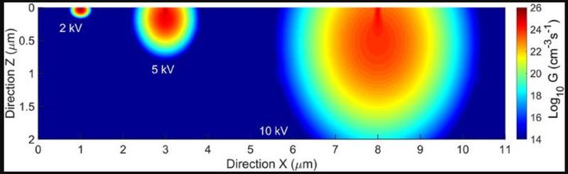
The model explores the improvements achievable in EBIC resolution when surface conditions of the specimens are carefully considered and optimized, and the ease of locating the pn-junction with a lower accelerated voltage and increased surface recombination velocity.
The paper also discusses the effect of surface band bending in the model, and the benefits of introducing controlled surface damage as a potential method for resolution enhancement via focused ion beam milling with Ga ions.