
High-precision atomic-scale strain mapping of nanoparticles from STEM images
Strain is a crucial factor which influences the physicochemical properties of nanoparticles. Being able to precisely measure strain is important in understanding the intrinsic mechanism of the enhanced performance of nanoparticles. Techniques which have been developed for strain analysis scanning transmission electron microscopy (TEM) images can be categorised into diffraction-based method and imaging-based method.
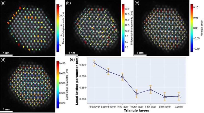
In the paper 'High-precision atomic-scale strain mapping of nanoparticles from STEM images' (published in Ultramicroscopy), the measured two-dimensional (2D) displacements from annular dark field (ADF) STEM images of a nanoparticle were found to be a good approximation to a projection of the actual three-dimensional (3D) displacements.
The paper presents a methodology for deformation analysis which is based on the detection of atomic columns from atomic-resolution STEM images in real space. Elastic deformation parameters (such as strain) are usually defined on the basis of a continuum of deformation.
The paper explores the appropriateness of various deformation parameters for atomic-scale investigation on STEM images, and presents a method for determining them. The team of researchers found that the local lattice parameter and principal strain components are the most physically meaningful parameters to express the materials distortion behaviour. Aside from the local lattice parameter, the other deformation parameters (such as normal strains, shear strains and displacements) heavily rely on the choice of reference lattice. The team found that different reference grids added a series of uniform offsets to these strain variants.
The paper also describes how the approach was applied to a PtCo3 bimetallic nanoparticle to quantify its deformation behaviour.