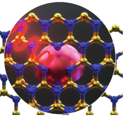
Defect engineering in wide bandgap two-dimensional materials
Optically active defects with ground state spins are a resource for optical quantum technologies, including quantum sensors and repeaters for optical networks. The most promising defects for these applications are systems that display promising optical and spin properties, such as room temperature optically initialised spin coherence, well-defined optical transitions that give rise to coherent single photon emission. These fundamental photophysical properties are dictated by the defect atomic structure, its symmetry, and coupling to the host material. While impressive work continues with the relatively small number of known defect systems in bulk crystals, in future we will need to engineer of the ideal defect platform for the application. For example, to realise scalable defect-based quantum optical technologies, it will be critical to engineer defects with optimal optical and spin properties and achieve deterministic creation of those defects.
This project will focus on defect engineering in a novel material platform – two-dimensional materials. The project will involve forming design principles for optimal optical and spin defects and routes towards their deterministic fabrication (including using a range of experimental tools, including ion, electron irradiation/implantation and laser writing). The project will involve developing the most promising defects towards new platforms for sensing and networking technologies via optically detected magnetic resonance experiments and device incorporation. The project will combine expertise in the department across defect engineering (Prof. Smith) and spin defects in hexagonal boron nitride (Prof. Stern) and will contribute to the UK-wide effort to develop new materials for quantum technologies.
Candidates will be considered in the January 2026 admissions field which has an application deadline of 08 January 2026.
Image: Igor Aharonovich