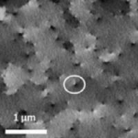
Electron channelling from wurtzite InAlN on SiC showing the threading dislocations (white circle)
Electron back scatter diffraction (EBSD) is now a ubiquitous tool for the characterisation of crystalline materials (grain orientations, phase identification, strain mapping). Electron channelling contrast imaging (ECCI) on the other hand is a method for imaging and characterising lattice defects (dislocations, stacking faults) that has slowly reached a level where it is now robust and reliable in producing impressive defect images. Added to this are the impressive results that can be obtained using thin foils and transmission imaging modes in SEM (TKD and bright/dark field imaging modes. The availability of good pattern and image simulations based on dynamical diffraction theory, and the possibility of advanced direct electron detection systems opens up new opportunities. Indeed, the EBSD detector can itself be thought of as a hugely versatile and adaptable source of multiple signal channels that can be combined in the many different ways to reveal different characteristics of the sample. Furthermore, SEM based imaging modes generally allow imaging of larger areas than is often the case in TEM and the possibility of serial sectioning via FIB or other routes, and in situ deformation/heating.
This project will continue our development of these methods and exploitation of the synergies between them and the use of multivariate statistical/machine learning routes for extracting more information describing the microstructure.

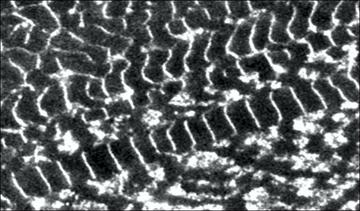
PSB structure in fatigued Cu
|

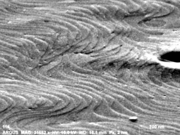
Atomic layer steps on GaN
|