
Solar cell processing via pulsed laser technology
Pulsed laser technology plays a crucial role in the fabrication of high-efficiency silicon solar cells, especially in enabling sophisticated architectures such as the interdigitated back contact silicon heterojunction cells. Realising precise laser processing for a wide range of applications in solar cell manufacturing requires an understanding of how the lasing operating parameters affect the materials and fabrications processes.
In the paper 'Nanosecond vs picosecond: the potential for advanced solar cell processing via pulsed laser technology', published in the Journal of Applied Physics, the authors contrast nanosecond and picsecond-pulsed UV lasers, and study their ability to enable laser-doped selective emitters and dielectric ablated openings, being two major methods for solar cell processing.
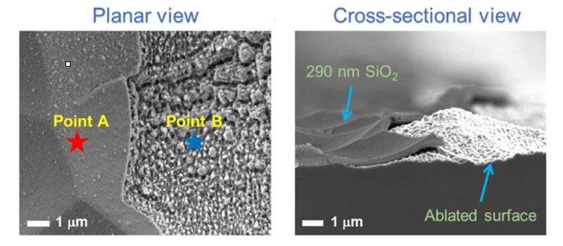
The lasers are operated in different power density regimes by controlling the pump current. In this paper it is shown that the nanosecond-pulsed laser offers great potential for doping, as implied from sheet resistance and dopant concentration profile measurements, but fails to produce melting-free ablation, even at very low fluences. Conversely, precise control of the picosecond laser allows damage-lean dielectric ablation but falls short of producing adequate doping concentrations for solar cell applications, even at high fluences. These results are discussed in the context of the fundamental mechanisms of laser-material interaction as a function of the pulse length.
The authors conclude that, via adequate pulse length and power density control, the same pulsed UV laser can be operated to fulfil the technical requirements of different processes in solar cell manufacturing toward high efficiency devices and improved yield.