
Oxide inversion layers and hot corona discharge
In the paper 'Enabling highly conductive charged oxide inversion layers through hot corona discharge', published in Solar Energy Materials and Solar Cells, the authors explain how they developed and used a hot-corona discharge technique, to facilitate the charge drive-in for a silicon solar cell, via a process which integrated corona discharging and thermal annealing into a single step.
They demonstrate in the paper that the process is effective in creating an n-type inversion layer on p-type silicon wafers, which yielded increases in carrier lifetime and reductions in emitter sheet resistance. The temperature (330-430oC) and time (30-1020s) dependence of this new hot-corona approach is presented.
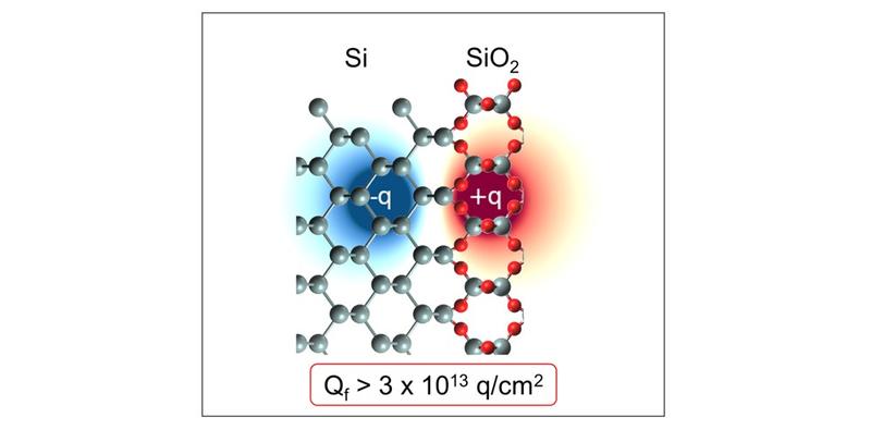
By optimising the process against temperature and ion drive-in cycles, the authors achieved the highest positive charge concentration reported on a SiO2/Si interface of >4.0x10¹³ q/cm2. With the ability to incorporate such high charge density, a low sheet resistance and highly conductive inversion layer can be formed. This represents a significant step forward in the attempt to replace the diffused emitter technology with a low-temperature alternative, enabling high efficiency inversion-layer solar cells with reduced thermal budget and intrinsic losses.