
Influence of Xe and Ga milling species
III-nitride materials, such as GaN and its alloys, are essential for modern microelectronics and optoelectronics due to their unique properties. Focused ion beam (FIB) techniques play a crucial role in their prototyping and characterisation at the micro- and nanoscale. Conventional FIB mills and Ga ions, however, present challenges, including surface amorphisation and point defect introduction, prompting the exploration of alternative ion sources.
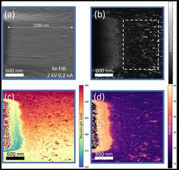
Xenon-based inductivity coupled plasma or plasma FIB has emerged as a promising alternative, offering reduced damage and better sample preservation. Despite extensive research on FIB-induced damage in GaN, systematic comparisons between Ga and Xe ion milling on the luminescence characteristics of GaN remain limited.
This study* aims to fill this gap by evaluating and comparing the extent of FIB-induced damage caused by Ga and Xe ions in wurtzite and zincblende GaN through cathodoluminescence measurements. The findings indicate that Xe ion milling yields higher integrated intensities compared to Ga ion milling, attributed to shallower implantation depth and reduced lattice disorder. The authors also observe a decrease in integrated intensity with increasing ion beam acceleration voltage for both wurtzite and zincblende GaN layers.
This study provides valuable insights into optimising FIB-based sample preparation techniques for III-nitride materials, with implications for enhancing device performance and reliability.
*'Influence of Xe and Ga milling species on the cathodoluminescence of wurtzite and zincblende GaN' as published in Journal of Applied Physics.