

RSB006 - Engineering Nanolayer Dielectrics for 2D Device Architectures
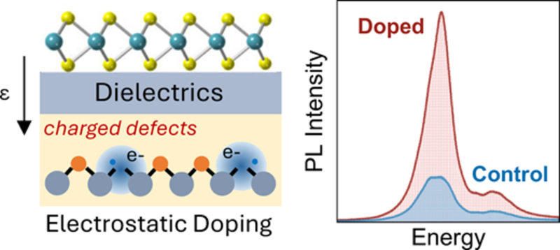
Two-dimensional (2D) semiconductors offer attractive properties for next-generation electronics, but their integration into practical devices is limited by the difficulty of controlling carrier concentration without damaging the material. Electrostatic doping using permanently charged dielectric nanolayers could provide a scalable route to engineer conductivity in 2D semiconductors, provided that the charge can be controlled, retained and patterned with nanoscale precision. (https://doi.org/10.1021/acsnano.6c07356)
This project will develop atomic layer deposition (ALD)-based dielectric nanolayers containing stable positive or negative charges. The student will investigate oxide materials and multilayer structures, including SiO₂, Al₂O₃, HfO₂ and ZrO₂, and establish methods for introducing and polarising ions within these films. Electrical and scanning-probe measurements will be used to quantify charge density, charge retention, permittivity, breakdown fields and the resulting nanoscale electric fields.
The project will then explore methods for controlling the lateral distribution of charge using lithographic and area-selective ALD approaches. Advanced Kelvin probe and electrostatic force microscopy will be used to map charged regions and interfaces, establish their spatial resolution and assess their stability. The resulting dielectric structures will provide design rules for non-volatile electrostatic doping and their integration into advanced 2D device architectures.
The work will contribute to the development of locally doped 2D materials, lateral diodes and high-performance p-type transistors for energy-efficient nanoelectronics.