


RSB005 - Atomic-scale Understanding of Copper Metallisation in Tandem Photovoltaic Devices
Interface and Electronic Materials Laboratory
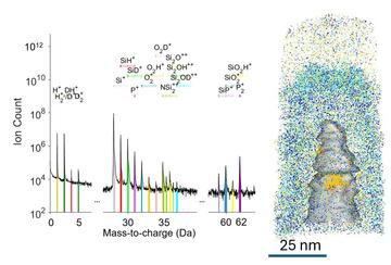
The replacement of silver with copper is an important route towards reducing the cost and material constraints of future photovoltaic manufacturing. However, copper can diffuse into semiconductor and passivating layers, alter metal/semiconductor interfaces and increase recombination, potentially limiting the efficiency and reliability of tandem solar cells. This project will investigate copper metallisation and its interaction with the nanoscale interfaces of perovskite/silicon tandem and advanced silicon photovoltaic devices.
Atom probe tomography (APT) will be used to determine the three-dimensional distribution of copper and other key elements across metal contacts, passivating contacts, tunnel layers and tandem interconnects, with near-atomic-scale chemical resolution. APT analysis will be combined with electron microscopy, photoluminescence, carrier-lifetime measurements, current–voltage characterisation and contact-resistivity measurements to connect elemental segregation and interfacial chemistry with charge transport and recombination losses. Where appropriate, thermal and electrical stress will be used to assess copper migration and contact stability.
The project aims to establish how copper processing conditions, diffusion and interfacial reactions influence photovoltaic performance, and to identify metallisation designs that provide low resistance, controlled interfaces and improved long-term stability. The outcomes will support scalable, silver-reduced metallisation strategies for high-efficiency tandem photovoltaics.

